In MEMS it is not uncommon to find centimeter-scale devices having functional elements at the micrometer level, particularly if the MEMS is a multiplexed system. There is a kind of MEMS that rely on high electric fields to function such as ion, electron, electrospray, and electrospinning sources. The implementation of a proximal annular gate structure surrounding each element substantially decreases the operational voltage of the array. However, even when a micro-sized gate is employed, the required voltages are still large—sometimes up to several kilovolts. Also, in order to reduce the leakage currents, the physical contact between the electrode and the substrate in high-voltage (HV) MEMS should be minimized and placed far away from the area where the high electric fields are present. The requirements on electrical insulation, operational voltage, and 3-D structure imply that the multiplexed MEMS cannot be easily fabricated using mainstream microfabrication technologies, which involve a single substrate and a series of selective deposition and removal of layers of material using a planar template via a lithographic process.
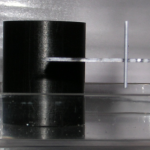
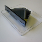
We have pioneered a packaging technology for HV MEMS that relies on DRIE-patterned meso-scaled deflection springs. The technology relies on the tight dimensional control of DRIE parts and the high structural performance of single crystal silicon to achieve MEMS-level assembly precision. The approach of using springs to assemble components is common in macroscale plastic goods, although without the same precision and repeatability that our technology can achieve. The dimensions of the springs and the forces exerted by them are such that it is feasible to hand-assemble the MEMS components. Other benefits of the assembly method are component process flow decoupling, optimization of each component substrate, modularity, larger overall device yield, and the ability to fabricate 3-D devices with out-of-plane dimensions well beyond what is achievable with thin-film processing. With the HV MEMS packaging technology we have been able to demonstrate alignment precision of the order of a few microns, and assembly repeatability of the order of a micron.
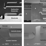
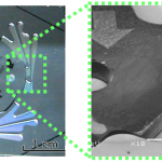
We first developed an out-of-plane implementation of the HV packaging technology, originally intended for a linear array of internally-fed electrospray emitters (Fig. 1), where the very high-aspect-ratio of the micro-channels led to the implementation of the emitters on the side of the wafer stack. The set of springs provide near perpendicular assembly between the electrodes and the main substrate (Fig. 2). The assembly is achieved using sets of springs etched on both substrates (Fig. 3). During assembly, the springs are set in tension to avoid buckling of the springs.
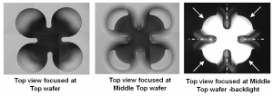
We have also developed an in-plane implementation of the assembly method (Fig. 4), where a disc-shaped object, i.e., twisting component, and a part that has a set of cantilever springs azimuthally distributed, i.e., main body, are assembled. The implementation was originally used in a planar array of externally-fed electrospray emitters, but we have also used the implementation to develop a high-pressure CNT-based electron impact ionizer. This implementation introduces several improvements over the design. First, the use of v-shaped notches to lock the spring tips prevents accidental disassembly and provides a reliable way to secure the assembly. Second, the spatial distribution of the springs provides high axial stiffness to tightly control the alignment of the assembly, but the lateral stiffness of the springs is small enough to accommodate differential thermal expansion between the two parts, or consistent over-/underetching of the sidewalls of the components during fabrication. Third, the springs are linearly tapered to achieve
stiffer springs that require less spring tip displacement to produce the same force. In this implementation, the twisting component is first roughly position into a recess on the top surface of the main body using as guides four protrusions. Then, the twisting component is rotated clockwise with respect to the main body. As the twisting component rotates, the springs are deflected. Finally, each spring tip falls into a notch etched on the edge of the twisting component to prevent further rotation, effectively locking the assembly. The choice of using an in-plane spring assembly could be perceived as unnecessary because of the availability of several wafer-bonding techniques. However, we strongly believe that spring-based methods are superior to other wafer-bonding methods to integrate electrode systems to high-voltage MEMS arrays for a number of reasons. First, the assembly is not permanent and can be remade multiple times, which allows design iteration and modular design. Second, spring-based assemblies give more freedom in the choice of substrates to be bonded, thus providing more flexibility to the design. Third, the assembly does not require high pressure or high temperature. Therefore, the assembly method does not impact the thermal budget of the device and also allows the use of temperature-degradable films and substrates such as polymer-based materials. Nevertheless, the assembly method is compatible with high-temperature processing. Fourth, the hand assembly step requires no special equipment, which improves manufacturing flexibility, at least at the research and development level.
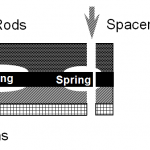
We have also implemented an HV packaging solution for out-of-plane MEMS QMFs (Fig. 5). In this case, sets of springs are etched into a four-wafer stack that is an assembly platform. The MEMS part includes a set of holes for the electrodes and spacers that are intended to be assembled by the system. The springs can be individually actuated using a handler. During assembly of the QMF, each spring is first fully deflected using the handler so the spring tip is not visible though the assembly hole that it controls (Fig. 6). Then, the part that is intended to be assembled is inserted into the assembly hole. Finally, the spring is released and the part is clamped. This implementation uses springs with handlers to avoid scratching the dielectric film on the spring surface, which is used as electrical insulation for the QMF. The performance that we obtained from these QMFs validates our estimates of alignment precision for the technology.
