
Current Collaborators: E. Heubel (MechE), A. I. Akinwande (EECS)
Funding: NASA
Ion energy measurements are an important aspect of a variety of experiments and technologies. From plasma thrusters and re-entry ablation assessment to fusion experiments and ion implantation for semiconductor doping, particle energy diagnostics provide valuable information. Through the use of CMOS processing technology, we have demonstrated an improvement in the current state-of-the-art concerning retarding potential analyzers (RPAs). For the first time, using in-plane assembly methods [1], grid alignments on the order of a few microns have been achieved. Furthermore, through wafer processing, micron-scale features are incorporated in batch-processed centimeter-scale devices [2].
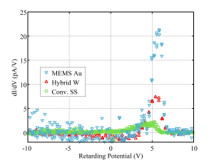
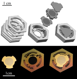
Our RPA consists of a fusion bonded six-wafer silicon assembly of curved springs that physically reference an electrode stack to tight tolerances (Figure 1). By utilizing 500μm-thick silicon grids, the device is made more robust to wear and can resist ablation and grid deflection. In combination with the 700μm-thick wafers used in the housing, this results in previously unattainable electrode spacing under 0.5mm [2][3]. We have achieved aperture sizes of 100μm, which in conjunction with the 200μm gap permit RPA use in plasmas with Debye lengths of 50μm or less. Thus far, preliminary tests have shown significant increases in detected ion currents despite decreased grid transparencies. The aperture/pitch sizes (and resulting transparencies) of the tested conventional-, hybrid- and MEMS-RPA are 152/280μm (26.7%), 100/150μm (40.3%), and 150/400μm (12.8%), respectively. Figure 2 reports measurements downstream of an ion source that show an order of magnitude increase in signal strength over conventional RPAs and a three-fold increase as compared to our hybrid-RPA. This phenomenon is attributed to the decreased ion interception of intermediate grids by our alignment methods.
References
[1] B. Gassend, L. F. Velásquez-García, and A. I. Akinwande, “Precision in-plane hand assembly of bulk-microfabricated components for high-voltage MEMS arrays applications,” Journal of Microelectromechanical Systems, vol. 18, no. 2, pp. 332-346, Apr 2009.
[2] E. V. Heubel, A. I. Akinwande, and L. F. Velásquez-García, “MEMS-Enabled Retarding Potential Analyzers for Hypersonic In-Flight Plasma Diagnostics,” Technical Digest of the Solid-State Sensor, Actuators and Microsystems Workshop, Hilton Head, SC, pp. 324-327, June 2012.
[3] I. H. Hutchinson, Principles of Plasma Diagnostics, 2nd ed. Cambridge: Cambridge University Press, 2002.