
Due to the exponential dependence on the field factor and hence the tip radius, emission currents are extremely sensitive to tip radii variation. Unfortunately, nanometer-sized tip radii in FEAs have a distribution with long tails such as Gaussian, lognormal, or Poisson. Therefore, spatial variation of the tip radius results in the spatial variation of the emission current and hence the current density. It also results in non-uniform turn-on voltages even for tips that are located next to each other.
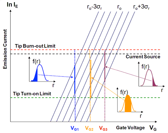
Figure 2 is a semi-log plot depicting a family of IV characteristics from a single tip for an FEA that has a tip radii distribution with average radius ro and radius variation σ. Each emitter current falls within the turn-on limit (controlled by the noise floor) and the burn-out limit (due to Joule heating). For a constant bias voltage only a small fraction of the field emitters in the array emits electrons because the sharper tips burn out early, before the duller tips emit, resulting in under-utilization of the FEA. Attempts to increase the emission current by increasing the voltage often result in emitter burnout and shifting of the operating voltage to higher voltages. Even though burning-out of the sharper tips of the FEA results in less emitter size variation and hence better emission uniformity, the larger average tip radius requires a larger bias voltage to produce the same current.
Consequently, alternative approaches for achieving uniform emission from FEAs have focused on control of the supply of electrons to the surface. In a metal the supply of electrons is very high, making the control of the supply challenging. However, in a semiconductor, where the doping level and the potential determine the local concentration of electrons, it is possible to configure the emitter such that either the supply process or the transmission process determines the emission current. Emission uniformity by controlling the supply of electrons to groups of emitters using ungated field effect transistors (FETs) or MOSFETs as ballasting elements have been reported in the literature. However, these approaches are not ideal because emission non-uniformity would still occur within the sub-set of emitters controlled by the same ballasting element. Individual control of the supply of electrons to each emitter would prevent destructive emission from the sharper tips while allowing higher overall current emission because of the emission of duller tips. Ballasting of individual emitters has not been attempted due fabrication complexity. Also, individual ballasting of Si emitters using classical MOSFETs results in small density of emitters per unit of area.
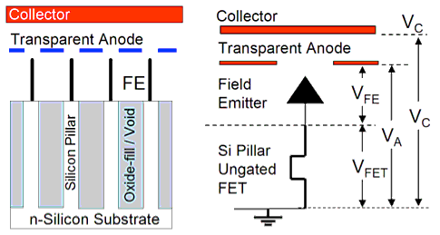
In this project we are exploring the use vertical ungated FETs to individually control the FEAs to achieve uniform and high current. A high aspect-ratio single-crystal Si column is a two-terminal ungated FET that can be fabricated using both deep reactive ion etching (DRIE) and thermal oxidation.
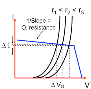
The two-terminal vertical ungated FET can easily be integrated with FEAs to create massive and dense arrays of individually ballasted field emitters that emit spatially uniform high currents, as shown in Fig. 3. If an ungated FET is used to control the current, the current uniformity depends on the magnitude of the output resistance of the FET, which is independent of the saturation current, so both low variation and high-current emission are achieved. The ungated FET has current source-like IV characteristics, i.e., it is able to simultaneously provide high current and high dynamic resistance for voltage drops across the FET larger than the saturation voltage, making it an ideal ballasting element to implement spatially uniform FEAs (Fig. 4).