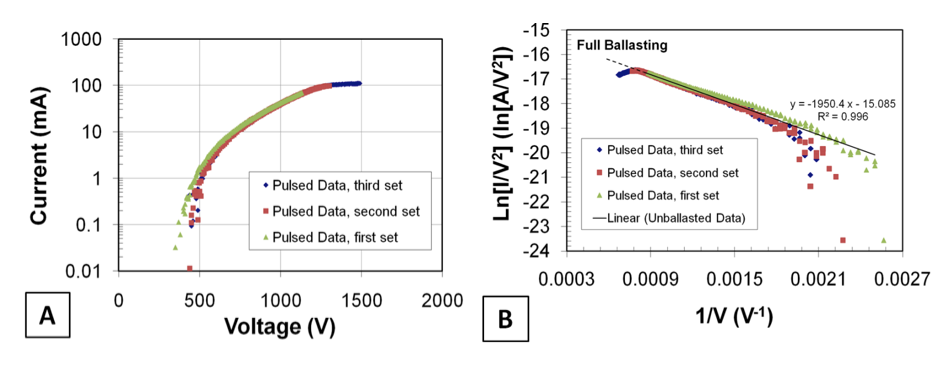
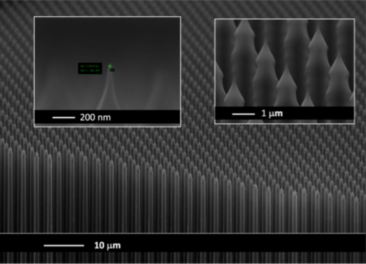
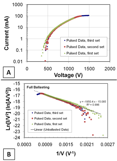
The vertical ungated FETs have current source-like IV characteristics due to the combination of the very high-aspect ratio of the structure, the doping level of the semiconductor, the bias voltage (pinch-off in the FET channel), and the velocity saturation of carriers at high fields in the semiconductor lattice. Using this technology, we have made massive individually ballasted FEAs (6.25-million emitters in 1 cm2, Fig 5). In the figure, the FETs are about 60 μm long and 0.8 μm wide. We have demonstrated experimentally demonstrated high current and current limitation at high voltages (Fig. 6). We have demonstrated currents in excess of 0.5 A (DC pulsed).