
Current collaborators: M. E. Swanwick, P. D. Keathley, R. G. Hobbs, Y. Yang, W. Graves, K. K. Berggren, F. X. Kärtner, L. F. Velásquez-García
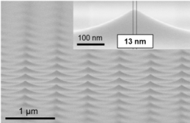
A collaboration of RLE and MTL investigators is creating the scientific and engineering knowledge for a compact coherent X-ray source for phase contrast medical imaging based on inverse Compton scattering of relativistic electron bunches. The X-ray system requires a low emittance electron source that can be switched at timescales of tens of femtoseconds or faster; the focus of our work has been the design, fabrication and characterization of massive arrays of a nanostructured high aspect-ratio silicon (Si) structures to implement low-emittance and high-brightness cathodes that can be triggered very fast using laser pulses to produce spatially uniform electron bunches. Si nanostructure arrays with highly uniform sub-10 nm tip radii have been fabricated via a combined optical lithography and diffusion limited oxidation technique. The fabrication process allows nanometer-level control over the dimensions of the electron emitter structures. Figure 1 shows an array of Si tips with 1.25 µm hexagonal pitch have an average radius of curvature of 6.2 nm and standard deviation of 1.1 nm (n=29); when the radius of curvature is changed to 21.6nm, the standard deviation remains approximately the same, i.e., 1.25 nm (n=69).
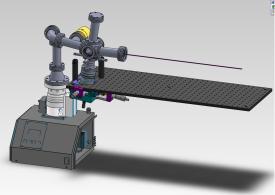
The tips are illuminated at a grazing incidence of roughly 84 degrees with a 1 kHz titanium sapphire laser (800 nm wavelength) with a pulse duration of 35 fs; the high electric field of the laser pulse is amplified by the silicon tips so the electrons can quantum tunnel from the tips into the vacuum. Experimental results using a time of flight spectrometer show electron beamlet array emission with 3-photon absorption [1]. Work is ongoing to optimize the tip geometry for both low emittance and high current. We are also designing and building a new vacuum chamber to test the devices (Figure 2). The chamber will pump down to 10-7 torr in ~15min with an anode bias up to 1100V.
References
[1] Keathley, Phillip D., William P. Putnam, Alexander Sell, Stephen Guerrera, Luis Velasquez-Garcia, and Franz X. Kaertner. “Laser Induced Annealing Dynamics of Photo-Electron Spectra from Silicon Field Emitter Arrays.” In CLEO: Science and Innovations, CM4L.7. OSA Technical Digest (online). Optical Society of America, 2012. http://www.opticsinfobase.org/abstract.cfm?URI=CLEO: S and I-2012-CM4L.7.